HBM4 and the Memory Wall in AI Accelerators
Why memory bandwidth, not FLOPS, bounds modern AI accelerators, and what the HBM3E to HBM4 transition changes — roadmaps, suppliers, tradeoffs.

Spend any time profiling a production LLM and the same uncomfortable fact surfaces: the expensive accelerator is idle most of the time. Not broken — waiting. Waiting on memory. The matrix engines that get the marketing finish their work and sit, starved, while weights crawl in from DRAM. This is the memory wall, and it’s the single most important thing to understand about why AI hardware looks the way it does in 2026.
HBM4 is the industry’s answer to that wall. This is a grounded read of what it changes, what it doesn’t, and who is actually shipping it — for engineers sizing infrastructure rather than reading press releases.
Why bandwidth, not FLOPS, is the binding constraint#
Start with the arithmetic, because the arithmetic is the whole argument.
A transformer generating text does it one token at a time. Each token requires streaming the model’s entire weight set from memory through the compute units, performing a relatively small number of operations on each value, and moving on. The ratio of compute to data movement — arithmetic intensity — is brutally low. At batch size 1, decode sits at roughly 1 to 2 FLOPs per byte moved for most transformer architectures.
Put that on a roofline and the conclusion is unavoidable: the decode phase lives far below the compute ceiling on essentially every GPU and model size. The chip cannot use the FLOPS it has because it cannot get data in fast enough. You are not compute-bound. You are bandwidth-bound, and adding FLOPS buys you nothing.
This is why two accelerators with similar peak FLOPS can serve tokens at wildly different rates: the one with more memory bandwidth wins the decode race. It’s also why batching helps — bundling requests reuses the same weights across multiple tokens, raising arithmetic intensity and pushing the workload back toward compute-bound territory. But batching trades latency for throughput, and there’s a ceiling to how much you can batch before tail latency breaks your SLA. For interactive serving — a chat endpoint, a coding assistant, a clinical summarizer behind a Hospital Management System — you live in the memory-bound regime whether you like it or not.
The takeaway for anyone doing AI implementation work: when serving is slow, measure bytes moved before you measure FLOPS. The bottleneck is almost always the channel, not the core.
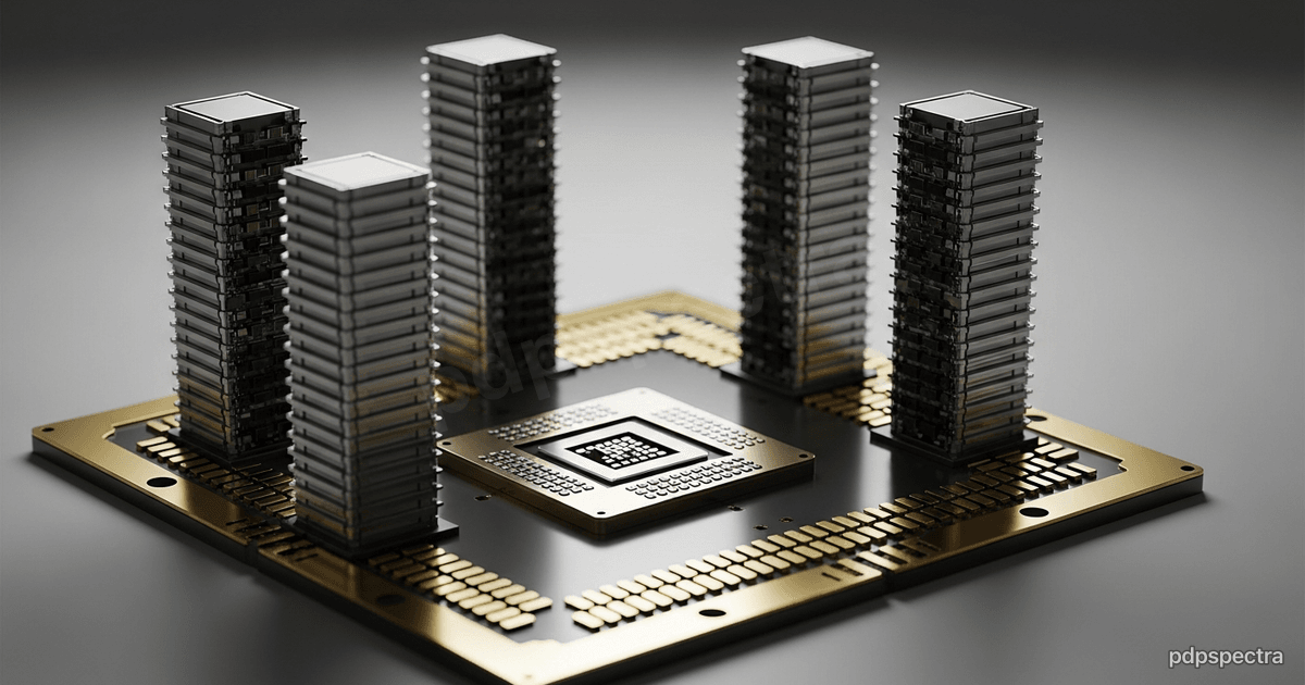
What HBM actually is#
High Bandwidth Memory solves the bandwidth problem with geometry, not clock speed. Instead of a few DRAM chips spread across a board talking over a narrow, fast bus, HBM stacks DRAM dies vertically, connects them with through-silicon vias, and sits the whole cube on a silicon interposer millimeters from the processor. The win is width: thousands of wires running at a modest clock beat a handful running fast, both for total bandwidth and for energy per bit.
That’s why every serious AI accelerator — NVIDIA’s, AMD’s, the hyperscalers’ custom silicon — uses HBM. It’s the only memory technology that keeps a modern matrix engine fed at all. The question is never whether to use HBM. It’s which generation, and how many stacks.
HBM3E to HBM4: what genuinely changes#
The headline change in HBM4 is structural, not just faster. JEDEC finalized the standard as JESD270-4 (JEDEC’s release), and the defining move is doubling the interface from 1024 bits to 2048 bits per stack.
That width doubling matters more than it sounds. Because the bus is twice as wide, you can hit higher aggregate bandwidth at a lower per-pin clock — which is easier on signal integrity and on power. Standard HBM4 transfer rates land up to roughly 8 GT/s, with vendors pushing toward 10 GT/s and beyond. The net is on the order of 2 TB/s per stack, a meaningful step over HBM3E.
Capacity moves in parallel#
HBM4 supports 4-high, 8-high, 12-high, and 16-high stacks, built from 24 Gb or 32 Gb DRAM dies, reaching up to 64 GB per stack at the 32 Gb 16-high configuration (JEDEC standard summary). Capacity is its own constraint, separate from bandwidth: bigger models and longer context windows need somewhere to put the weights and the KV cache, and HBM is the only memory close enough to matter. The taller the stack, the harder the thermal and yield problem — which is exactly where the suppliers are differentiating.
The base die goes to a logic foundry#
This is the change most coverage underplays. In HBM4, the base die — the logic layer at the bottom of the stack that talks to the processor — moves onto advanced logic process nodes from a foundry. TSMC is manufacturing HBM4 base dies on logic-class nodes such as N5, with 3nm base dies on the roadmap for HBM4E.
The implication is bigger than a spec bump. A logic-process base die means you can put real logic in the memory stack — caches, custom interface blocks, application-specific features. “Custom HBM” stops being a slogan and becomes a design lever: a buyer like NVIDIA can co-design the base die with the GPU. Memory and compute start to blur at the package boundary. That’s an architectural shift, not a generational refresh.
Where Rubin lands#
Concretely: NVIDIA’s Rubin GPU pairs eight HBM4 stacks for up to 288 GB per GPU and up to 22 TB/s of bandwidth (Tom’s Hardware roadmap). Set that against the memory-wall argument and the design intent is obvious: the largest single jump Rubin makes over Blackwell is bandwidth and capacity, because that’s what unblocks decode. The FLOPS get the slide; the HBM4 does the work.
The suppliers: a three-way fight#
HBM4 is supplied by exactly three companies, and the competition between them is one of the defining stories of the 2026 hardware cycle (EE Times from CES 2026).
SK Hynix has led recent HBM generations and is pressing on density, targeting mass production of its 16-high HBM4 in the second half of 2026. Samsung is pushing volume early, with 12-high HBM4 shipments and aggressive transfer-rate claims. Micron is scaling 12-high, 36 GB parts on the 2048-bit interface and expanding HBM4 wafer capacity through the year. All three delivered HBM4 samples to NVIDIA ahead of contract finalization, because qualifying into the Rubin supply chain is the prize that funds the next node.
For buyers, the three-supplier reality has a practical edge: HBM is the gating component for AI accelerator supply. When GPUs are scarce, it’s frequently HBM yield — not the logic die — that’s the constraint. If you’re forecasting capacity for a Data Platforms or Operational Automation build that leans on GPU inference, the memory supply chain is a risk line in your plan, not a footnote.
What this means if you don’t build silicon#
You don’t fab accelerators. You still inherit every one of these decisions through the instances you rent and the models you serve. Three durable rules fall out of the memory wall:
- Buy bandwidth and capacity, not headline FLOPS. For inference, the spec that moves your cost-per-token is HBM bandwidth and how much model plus KV cache fits in memory. Compare accelerators on those first.
- Quantization is a bandwidth play, not just a size play. Dropping weights from FP16 to INT8 or INT4 doesn’t only shrink the model — it cuts the bytes you stream per token, so the bandwidth-bound decode step speeds up roughly in proportion. That’s why quantization buys latency, not just memory headroom.
- Watch capacity as hard as bandwidth. Long-context workloads are gated by how much KV cache fits in HBM. A model that runs at short context can fall off a cliff at long context when the cache spills. Size for the context length you actually serve.
The memory wall isn’t going away. HBM4 raises it — wider interface, taller stacks, a logic-process base die that opens the door to genuine memory-compute co-design — but the fundamental asymmetry between how fast we can compute and how fast we can move data is the permanent condition of this field. The engineers who internalize that build serving stacks that age well. The ones who chase FLOPS keep buying chips that sit idle, waiting.
Sizing inference infrastructure and tired of comparing accelerators on the wrong number? Talk to pdpspectra about building serving stacks that respect the memory wall.