Chiplets and Advanced Packaging: The New Moore's Law
Monolithic dies hit the reticle limit years ago. Chiplets, CoWoS interposers, and the UCIe standard are how leading-edge silicon keeps scaling in 2026.

For five decades the performance story was simple: shrink the transistor, double the count, ship a faster monolithic die. That story is over at the high end. The single largest die a lithography scanner can print in one exposure — the reticle limit — sits at roughly 858 mm² for a standard EUV field, and the most demanding AI accelerators blew past it years ago. You cannot make the die bigger. The exposure field physically will not allow it.
So the industry did what every mature engineering discipline does when a primitive caps out: it stopped trying to build one big thing and started composing several smaller things. Chiplets and advanced packaging are now where the performance scaling actually happens. The interconnect between dies, not the transistor inside them, is the constraint that matters most in 2026.
The reticle wall is a hard physical limit#
A photolithography scanner images a single reticle field onto the wafer, steps over, and repeats. The maximum field is fixed by the optics. For leading-edge EUV that field tops out near 858 mm², and TSMC works to a practical ceiling slightly below that. A modern flagship GPU compute die already presses against this number. There is no clever process trick that prints a 1,200 mm² monolithic die in one shot — the lens does not cover it.
Yield makes the wall worse than it looks. Defect density is roughly constant per unit area, so the probability that a die is defect-free falls fast as the die grows. Double the die area and you do not just halve the number of candidates per wafer — you also slash the fraction of them that work, because each one now spans more potential defects. A reticle-sized monolith on a leading node can yield catastrophically. The economics punish size brutally.
Chiplets attack both problems at once. Split the design into smaller dies — a compute tile, an I/O tile, a cache tile — and each one yields far better because it is small and because you can fabricate it on the process node that suits it. Compute logic goes on the bleeding-edge node; I/O and analog, which gain little from shrinking, stay on a cheaper mature node. You assemble the working dies, discard the bad ones before packaging, and only pay leading-edge prices for the silicon that genuinely needs it. The yield math flips from punishing to favourable.
CoWoS, interposers, and silicon bridges#
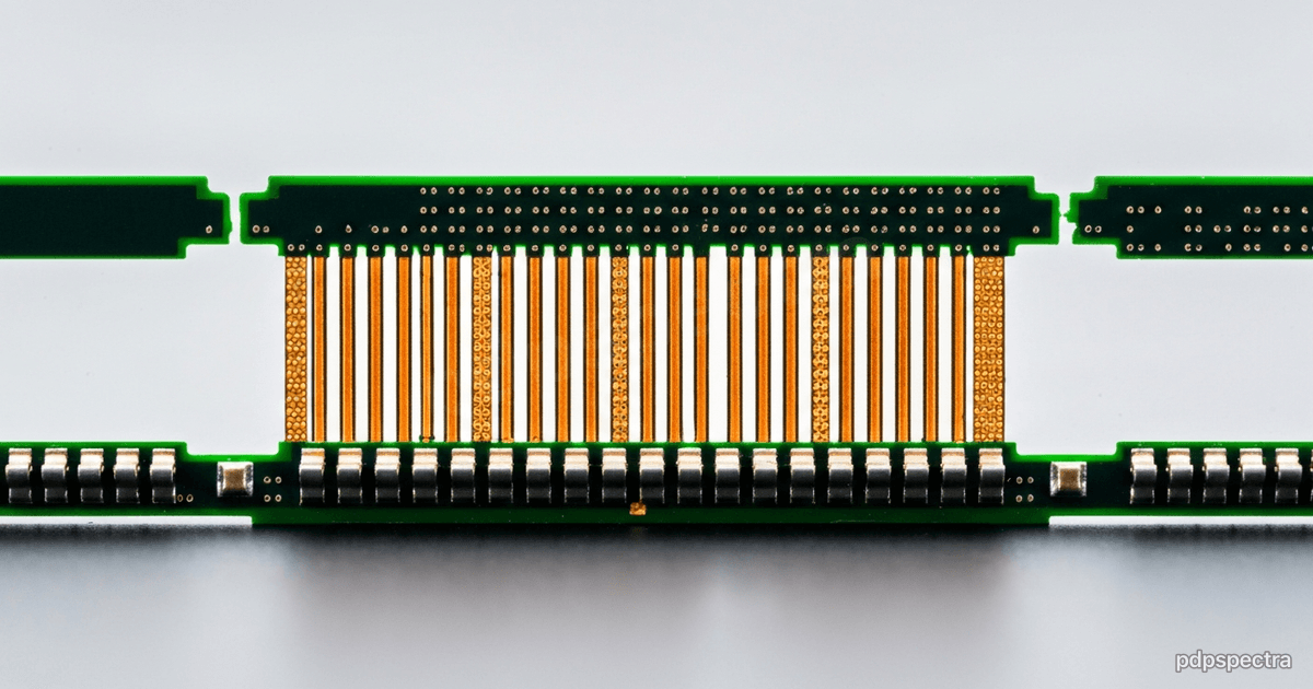
Splitting the die is the easy half. The hard half is reconnecting the pieces with enough bandwidth that the package behaves like one chip. That is the job of advanced packaging, and TSMC’s CoWoS — Chip-on-Wafer-on-Substrate — is the workhorse for AI silicon.
In classic CoWoS-S, the dies sit on a large silicon interposer: a passive slab of silicon carrying tens of thousands of fine wires that route signals between dies and out to the package. Because the interposer is silicon, it supports microbump pitches far tighter than any organic substrate, which is what makes wide HBM memory interfaces possible. The catch is that the interposer itself must be manufactured, and a large interposer is itself constrained by — you guessed it — the reticle. TSMC stitches multiple exposures to build interposers several times the single-field size; current Super Carrier generations reach roughly nine reticle areas, carrying a dozen HBM stacks alongside the compute dies, as Tom’s Hardware has reported.
Hauling a full-size silicon interposer under every package is expensive and warps under thermal stress. The answer is CoWoS-L, which replaces the monolithic interposer with a cheaper substrate plus small silicon “bridges” — local silicon interconnect — embedded only where two dies actually need a dense connection. You get interposer-class wiring density exactly where it matters and ordinary substrate everywhere else. Intel’s EMIB uses the same idea of an embedded bridge. This is the direction the whole industry is moving, because it scales package size without scaling interposer cost linearly.
TSMC’s published roadmap pushes this hard: the next CoWoS generations target packages beyond 14 reticle areas by the end of the decade, carrying twenty-plus stacked compute chiplets and two dozen HBM stacks. The performance curve the industry once got from transistor scaling now comes substantially from making the package bigger and the inter-die links faster.
UCIe: the die-to-die standard that makes chiplets a market#
Chiplets inside a single vendor’s package are old news — AMD shipped multi-die CPUs for years. The genuinely new thing is the prospect of a chiplet ecosystem: buying a compute tile from one vendor, an I/O tile from another, and a specialised accelerator tile from a third, then composing them in one package. That only works if everyone agrees on how dies talk to each other. That agreement is UCIe — Universal Chiplet Interconnect Express.
UCIe defines the die-to-die physical layer, protocol, and link management so that a die from vendor A can be bonded next to a die from vendor B and they interoperate. The UCIe 2.0 specification, released in 2024, added a manageability layer — a dedicated control plane to configure, test, and monitor each chiplet independently of the data path, which is what you need to actually debug a heterogeneous package in production. The consortium has since advanced the specification further, extending toward 3D hybrid-bonded stacks where bump pitches drop toward a single micron.
The strategic point is that UCIe turns packaging from a vertically integrated dark art into something closer to a components market. If you have ever assembled a Data Platform out of best-of-breed services rather than one monolith, the logic is identical: standard interfaces let you compose specialised parts and replace any one of them without rebuilding the whole. Silicon is now learning the lesson that software architecture learned a decade ago.
Why the interconnect is the new bottleneck#
Once the package is a network of dies, the link between them dominates. Three quantities decide whether a chiplet design is any good:
- Bandwidth density — bits per second per millimetre of die edge. HBM and wide die-to-die buses live or die on this.
- Energy per bit — picojoules to move one bit across the link. At AI-accelerator scale this is a meaningful fraction of total power, and shorter, denser links across a silicon bridge beat long traces across an organic substrate by a wide margin.
- Latency — every die crossing adds nanoseconds, and software that assumes a flat memory model will fall off a cliff when it does not account for the topology.
This is why advanced packaging capacity, not wafer capacity, became the throttle on AI hardware supply. The leading-edge transistors were available; the CoWoS lines to assemble them into a working accelerator were not. TSMC has spent 2025 and 2026 aggressively expanding packaging throughput precisely because that is where the line forms.
Known-good-die and the cost of testing late#
There is a failure mode that haunts chiplet economics: you cannot package a bad die and find out afterward. If you bond ten dies onto an expensive interposer and one of them is defective, you have not lost one cheap die — you have lost the whole assembly, interposer and HBM stacks included. That is the most expensive way possible to discover a fault. The discipline that prevents it is known-good-die testing: every chiplet is tested thoroughly before it goes into the package, so only verified-working dies are committed to assembly.
This sounds obvious and is brutally hard in practice. Testing a bare die at speed, before it has a package to mount in or pins to probe, demands sophisticated test access — which is part of why the UCIe manageability layer matters, since it standardises a path to test and monitor each die in isolation. The principle generalises far beyond silicon: validate each component at the cheapest possible stage, because the cost of catching a defect rises by an order of magnitude at every integration step you let it slip past. Anyone who has paid to debug a bad record in production rather than at ingestion knows the shape of this curve exactly.
Thermal density is the quiet constraint#
Packing more compute dies and HBM into one package concentrates heat into a smaller footprint, and the power envelopes are climbing into territory that air cooling simply cannot serve. The largest multi-die accelerators now assume liquid cooling as a baseline, not an option, which is why so much of the 2026 data-centre build-out is really a plumbing and thermal-engineering problem dressed up as a silicon one. The package can only deliver its rated performance if the heat can actually get out, and at these densities that is no longer a given.
What this changes for systems built on top#
It is tempting to file all of this under “foundry problems.” It is not. The shift to chiplet-based accelerators changes the hardware your workloads actually land on, and the effects reach all the way up to AI implementation decisions.
Memory bandwidth per package is climbing far faster than raw compute, because each new interposer generation bolts on more HBM stacks. Workloads that were compute-bound are increasingly memory-bound on this hardware, which rewards careful attention to data layout and batching. The non-uniform topology inside a multi-die package means that, much like a N2-class compute die, peak numbers on a spec sheet only materialise if your software respects where the data lives. For anyone running large models behind, say, a Hospital Management System’s clinical-summarisation feature, the practical lever is matching batch sizes and sequence lengths to the memory hierarchy of whatever accelerator you actually rent — the gap between naive and tuned utilisation is large and entirely yours to capture.
The broader lesson is architectural, and it is the one worth keeping. When a primitive stops scaling, you do not keep pushing the primitive — you compose around it with standard interfaces and pay only for the parts that need the expensive process. That is true of silicon dies, and it is just as true of the systems we build on top of them.
Building on accelerators you don’t control? We tune AI implementation and Data Platforms to the real hardware underneath — not the spec sheet. Talk to our engineers.