Gate-All-Around and the Angstrom Era of Silicon
FinFET is out of road. GAA nanosheets, backside power delivery, and High-NA EUV are how foundries push past 2nm into the angstrom era in 2026.

The FinFET ran for more than a decade and carried the industry from roughly 22nm down through the 3nm-class nodes. It is now out of road. At the dimensions leading-edge logic operates in for 2026, the fin geometry can no longer hold the channel under control — leakage creeps up, the gate loses authority over the current it is supposed to switch, and the easy density gains evaporate. So the foundries did what they did when planar transistors ran out: they changed the transistor.
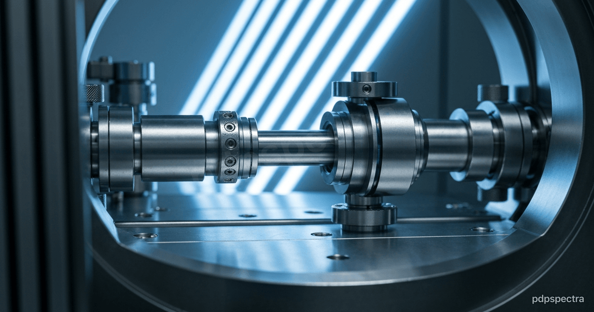
The replacement is the gate-all-around nanosheet, and its arrival marks the start of what the industry has taken to calling the angstrom era — nodes named in tenths of a nanometre rather than whole nanometres. The naming is marketing; the engineering underneath is real, and it rests on three changes happening at once: the transistor structure, where the power comes in, and how the patterns get printed.
From fin to nanosheet: why the gate had to wrap#
A transistor switches by using a gate to control a channel. The more sides of the channel the gate touches, the better it controls the current and the less the device leaks when it is supposed to be off. The planar transistor touched one side. The FinFET stood the channel up as a fin and wrapped the gate around three sides, which bought a decade of scaling. The gate-all-around nanosheet finishes the job: it stacks the channel as several thin horizontal sheets and wraps the gate completely around all four sides of each one.
That total enclosure is the entire point. Wrapping the gate on all sides cuts leakage and lets the device run at lower voltage, which is where power savings come from at constant performance. It also gives designers a new knob the FinFET never had: nanosheet width. A fin has a fixed height, so you tune drive strength in quantised steps by adding whole fins. A nanosheet can be drawn wider or narrower, so you tune drive current continuously. That flexibility matters for squeezing both high-performance and low-power cells out of the same process.
The transition is not theoretical. TSMC moved its N2 node into volume production on nanosheet transistors, with the foundry citing improvements in the mid-teens percentage range at equal power — the first time it has shipped a non-FinFET architecture on its main line. Samsung moved to gate-all-around earlier at its own 3nm-class node, and Intel built its 18A node on a nanosheet device it calls RibbonFET. The architecture that will define logic for the rest of the decade is now in production at all three leading-edge foundries. We covered the N2 ramp and the competitive picture in detail; here the focus is the device physics and what comes after.
Backside power delivery: moving the wiring out of the way#
The second change is less visible and arguably harder. For the entire history of the integrated circuit, both signal wires and power wires have been routed on the same side of the silicon — stacked above the transistors in the metal layers. As transistors shrank, that became a traffic jam: fat power rails and thin signal wires fighting for the same congested space, with the power network robbing the signal network of room and the resistance of long thin power wires causing voltage to droop before it reaches the transistors.
Backside power delivery splits the two apart. The power network moves to the underside of the wafer, leaving the top side free for signal routing alone. Intel productised this as PowerVia and was first to ship it, and the benefits are concrete: the power interconnects can be made fatter and therefore less resistive, voltage droop falls, and the decongested signal layers allow tighter logic packing. It is one of those rare changes that helps power, performance, and density simultaneously.
TSMC’s implementation arrives a step later. The A16 node, targeted for production toward the end of 2026, pairs nanosheet transistors with a backside power rail TSMC calls Super Power Rail — a more aggressive scheme that connects power directly to the transistor source and drain rather than through an intermediate contact. It is harder to manufacture, which is exactly why it lands a generation after the first nanosheet node rather than alongside it. Decoupling the two transitions — change the transistor first, add backside power second — is a sane risk-management decision, and it tells you something about how the foundries sequence their bets.
Why these two changes are sequenced, not stacked#
It is worth dwelling on the sequencing, because it is an engineering lesson that generalises. Both gate-all-around and backside power are disruptive, yield-threatening transitions on their own. Stacking them into one node multiplies the risk: when something goes wrong you cannot tell which change caused it. Introducing nanosheets first, stabilising the process, then layering backside power onto the following node, keeps each change independently debuggable. The nanosheet structure itself opens room for these power and contact innovations, but room is not the same as a working process. Anyone who has shipped a hard migration — a database engine swap, a Data Platform re-architecture — knows the instinct: change one load-bearing thing at a time so failures stay attributable.
Design-technology co-optimisation: the gains nobody photographs#
There is a third source of improvement that gets none of the attention the transistor and the lithography do, and it increasingly matters more than either: design-technology co-optimisation, or DTCO. Past a certain point you stop getting density from shrinking the transistor and start getting it from drawing the standard cells more cleverly — reducing the number of routing tracks a cell occupies, sharing contacts, packing the library so logic fits in less area at the same transistor dimensions. Backside power feeds directly into this, because clearing the power rails off the top frees routing tracks the cell designer can reclaim.
This is why two foundries on nominally similar nodes can ship meaningfully different density and power. The headline node name captures the transistor; it says nothing about how well the cell library and the routing were co-designed around it. For anyone evaluating which process a product should target, the spec-sheet node number is the least informative figure in the conversation. The gains that show up in a shipping product come from the unglamorous co-optimisation work, not the number in the marketing name.
High-NA EUV: printing patterns the old optics cannot resolve#
The third change is in the lithography itself. You cannot keep shrinking features if you cannot print them, and standard EUV scanners — built around optics with a numerical aperture of 0.33 — are running into their resolution limit. The fix is High-NA EUV: a new generation of ASML scanners with a numerical aperture of 0.55 that resolve substantially finer features in a single exposure, avoiding the cost and alignment penalty of splitting a pattern across multiple exposures.
These machines are enormous, cost on the order of hundreds of millions of dollars each, and shipped first to Intel, which completed acceptance testing of an ASML High-NA system in early 2026 as it pushes toward its 14A node. Intel has signalled risk production on 14A around late 2026 with high-volume manufacturing in the 2027 to 2028 window. The strategic gamble is real: High-NA is ferociously expensive, and a foundry that adopts it early either leapfrogs competitors who waited or eats the cost of being the one debugging the tooling for everyone else. TSMC has been more measured, leaning on multi-patterning with proven 0.33-NA optics for as long as the economics favour it.
The disagreement is itself informative. Two of the most capable engineering organisations on the planet look at the same physics and the same price tag and reach different answers on timing. That is what a genuine frontier looks like — not a settled roadmap, but a live argument about cost, risk, and yield.
What the angstrom era actually buys you#
Strip away the node names and the gains are incremental per generation: a chunk of performance-per-watt here, a density improvement there. Nobody is doubling anything overnight anymore. The angstrom era is a story of compounding small wins, each one extracted at rising capital cost, each one demanding a harder process change than the last.
For anyone running real workloads, the takeaway is not which foundry wins. It is that the efficiency floor under your compute keeps dropping, slowly and reliably — every model you serve, every batch job in a Data Platform, every inference behind a School ERP’s analytics dashboard rides on transistors that get modestly cheaper to run each generation. The hardware will keep handing you gains. Whether your AI implementation actually captures them, rather than leaking them to lazy batching and idle accelerators, is the part that stays firmly in your hands.
Squeezing real efficiency out of modern silicon takes more than renting it. We engineer AI implementation and Data Platforms that capture the hardware’s gains instead of leaking them. Talk to our engineers.