NVIDIA Rubin: What Comes After Blackwell
What's publicly known about NVIDIA's Rubin GPU, Vera CPU, the NVL72 rack, HBM4 memory, and the NVLink direction. Verified, not hyped.

Blackwell is barely warm in production racks and NVIDIA has already named its successor. At CES and GTC 2026, the company laid out Rubin — a new GPU, a new Arm CPU called Vera, and a rack-scale system that treats 72 GPUs as one machine. If you plan AI infrastructure for a two-year horizon, Rubin is the curve you’re buying against whether you deploy it or not.
This piece is a sober read of what NVIDIA has actually disclosed, separated from what it hasn’t. Vendor launch numbers are vendor launch numbers — measured under conditions NVIDIA chose, in a precision format NVIDIA defined. We’ll take them at face value where they’re confirmed and flag where they’re projection. That distinction is the whole job of anyone doing real AI implementation planning rather than reading slides.
The naming, and why the system is the product#
Rubin is the GPU. Vera is the CPU. “Vera Rubin” is the platform that bolts them together, and the unit NVIDIA wants you to buy is neither chip alone — it’s the rack.
NVIDIA describes the Rubin generation as six new chips: the Rubin GPU, the Vera CPU, an NVLink 6 Switch, the ConnectX-9 SuperNIC, the BlueField-4 DPU, and the Spectrum-6 Ethernet switch. That list is the real architecture statement. The GPU is no longer the product. The product is a co-designed system where memory, scale-up fabric, scale-out networking, and data movement are specified together. You don’t get to mix and match the good parts.
This is the same lesson that governs any serious Data Platforms build: the bottleneck is rarely the compute node in isolation, it’s the seams between nodes. NVIDIA has internalized that and is selling the seams.
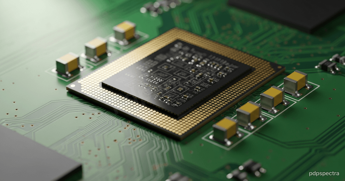
The Rubin GPU: what’s confirmed#
The Rubin GPU is built from two reticle-sized dies on TSMC’s 3nm-class process, carrying a combined 336 billion transistors per NVIDIA’s developer briefing. For reference, Blackwell was a roughly 208-billion-transistor design on TSMC’s 4NP node, so Rubin is both a full process shrink and a larger transistor budget.
On throughput, NVIDIA quotes up to 50 petaFLOPS of NVFP4 inference and 35 petaFLOPS of NVFP4 training per GPU, framed on its slides as roughly 5x and 3.5x Blackwell. Read NVFP4 carefully: it’s NVIDIA’s 4-bit floating-point format, and these figures are not comparable to FP8 or BF16 numbers from another vendor. A “5x” that depends on a narrower datatype is a real gain for workloads that tolerate 4-bit, and a marketing artifact for workloads that don’t. Know which of your models is which before you size anything.
Memory is the headline NVIDIA buries#
The line that should get your attention isn’t the FLOPS. It’s the memory. Rubin moves to HBM4, with NVIDIA citing up to 288 GB per GPU and up to 22 TB/s of memory bandwidth (Tom’s Hardware roadmap coverage). For autoregressive inference — the token-at-a-time decode path that dominates production LLM serving — bandwidth, not FLOPS, sets the pace. We’ve written separately about why the memory wall, not the compute roofline, bounds modern accelerators. Rubin’s bandwidth jump is the spec that actually changes serving economics.
Vera: NVIDIA’s own CPU grows up#
Grace was NVIDIA’s first serious data-center CPU. Vera is the second swing, and it’s a custom-core design rather than a licensed Arm Neoverse build.
NVIDIA specifies Vera with 88 custom Arm “Olympus” cores running 176 threads, full Armv9.2 compatibility, roughly 227 billion transistors, and up to 1.5 TB of LPDDR5X memory delivered through SOCAMM modules at up to 1.2 TB/s (VideoCardz’s NVL72 breakdown). The CPU and GPU are stitched together over NVLink-C2C at 1.8 TB/s of coherent bandwidth, so the GPU can reach host memory without crawling across PCIe.
The strategic point: NVIDIA designs the CPU now so it can keep the GPU fed and stop paying the PCIe tax. The Vera-to-Rubin coherent link is the difference between a CPU that hosts the GPU and a CPU that’s an extension of it. For anyone building Operational Automation pipelines where pre- and post-processing live on the CPU and the model lives on the GPU, that coherent path is where latency quietly disappears.
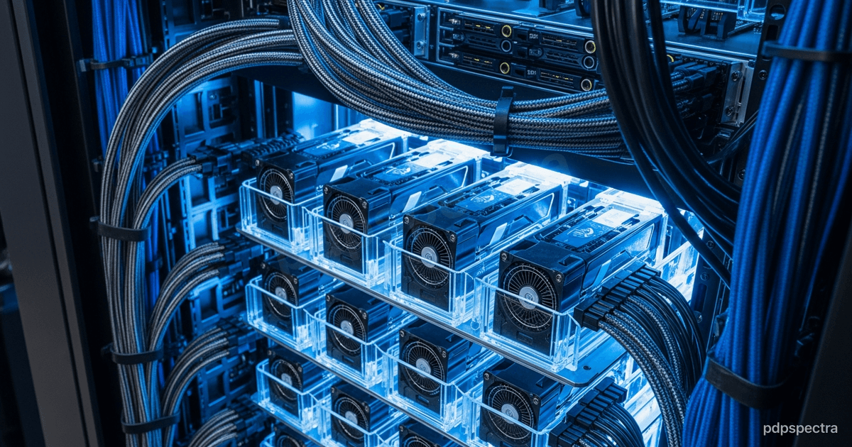
The rack is the computer: Vera Rubin NVL72#
Here’s where the “system, not chip” thesis becomes concrete. The flagship configuration is the Vera Rubin NVL72: 72 Rubin GPUs and 36 Vera CPUs in a single liquid-cooled rack, wired together with NVLink 6 so the whole rack presents as one large accelerator.
NVIDIA’s figures for the rack (its product page and DCD’s CES keynote report):
- 3.6 exaFLOPS of NVFP4 inference and 2.5 exaFLOPS of NVFP4 training
- 20.7 TB of HBM4 capacity and 54 TB of LPDDR5X across the rack
- 1.6 PB/s of aggregate HBM bandwidth
- 3.6 TB/s of NVLink bandwidth per GPU, 260 TB/s of scale-up bandwidth across the rack
That 260 TB/s scale-up number is the one to internalize. NVLink 6 is what lets 72 GPUs behave like one device with a shared, coherent view of memory — and the reason NVIDIA can sell the rack as the atomic unit of purchase. The exaFLOPS headline depends on NVFP4 and on NVIDIA’s measurement conditions; the interconnect bandwidth is the more architecturally honest figure, because it’s the thing that determines whether a model too big for one GPU runs well across many.
Why this matters beyond the hyperscalers#
You are probably not buying an NVL72 rack. But the architecture it represents — coherent memory across dozens of accelerators, CPU and GPU co-designed, the network treated as a first-class component — is the template the entire industry now copies down-market. The cloud instances you’ll rent in 2027 inherit these decisions. A regional clinic running inference behind a Hospital Management System, or a vendor serving a multi-tenant School ERP, will touch Rubin-class hardware through an API long before they touch the rack. The design choices upstream still set your cost-per-token downstream.
What is NOT confirmed — and where to stay skeptical#
This is the section most launch coverage skips. Being specific about the unknowns is the difference between planning and guessing.
Real-workload performance. Every throughput figure above is NVFP4 under NVIDIA’s conditions. Independent MLPerf results on shipping Rubin silicon — the only numbers that survive contact with your workload — were not available at the time of writing. Treat the 5x framing as a ceiling, not a forecast.
Timeline. NVIDIA stated Rubin reached full production in Q1 2026, ahead of earlier guidance that pointed at the second half of the year. Broad partner and cloud availability is still described as second-half 2026. “Full production” and “you can rent it” are different milestones; plan against the latter.
Power and cooling. NVL72-class density is liquid-cooled for a reason. Per-GPU and per-rack power envelopes drive the facilities question — and for most teams the real constraint on adopting Rubin won’t be silicon supply, it’ll be whether the data center can cool it. Confirm the power numbers for the specific SKU you intend to deploy; do not extrapolate from the rack headline.
Pricing. No credible per-unit pricing is public. Anyone quoting you a number is guessing.
How to actually plan against this#
Three moves, none of which require owning Rubin.
- Profile your workload’s datatype tolerance now. If your serving path tolerates 4-bit, Rubin’s NVFP4 gains are real money. If it doesn’t, you’re buying memory bandwidth and interconnect, not FLOPS — which may still be the right buy.
- Design for bandwidth, not peak compute. The architecturally durable wins in Rubin are HBM4 capacity and NVLink 6 scale-up. Build your serving stack so it benefits from bandwidth and coherent memory, because that’s what the next three generations keep improving.
- Wait for MLPerf before committing budget. Vendor numbers tell you the shape of the gain. Independent benchmarks tell you the size. Commit on the second.
Rubin is a real and significant step — a process shrink, HBM4, a serious custom CPU, and a rack-scale fabric that makes 72 GPUs act like one. It is also a launch narrative, measured in a format NVIDIA chose. Both things are true. The engineering discipline is holding both in your head while you plan.
Planning an accelerator refresh and trying to separate the spec sheet from the workload? Talk to pdpspectra about right-sizing AI infrastructure against your actual serving profile.